EMC电磁兼容和可靠性分析仪器、仪表、设备综合服务供应商
芯片级、板级、系统级ESD静电抗扰和EMI电磁干扰测试方案定制商

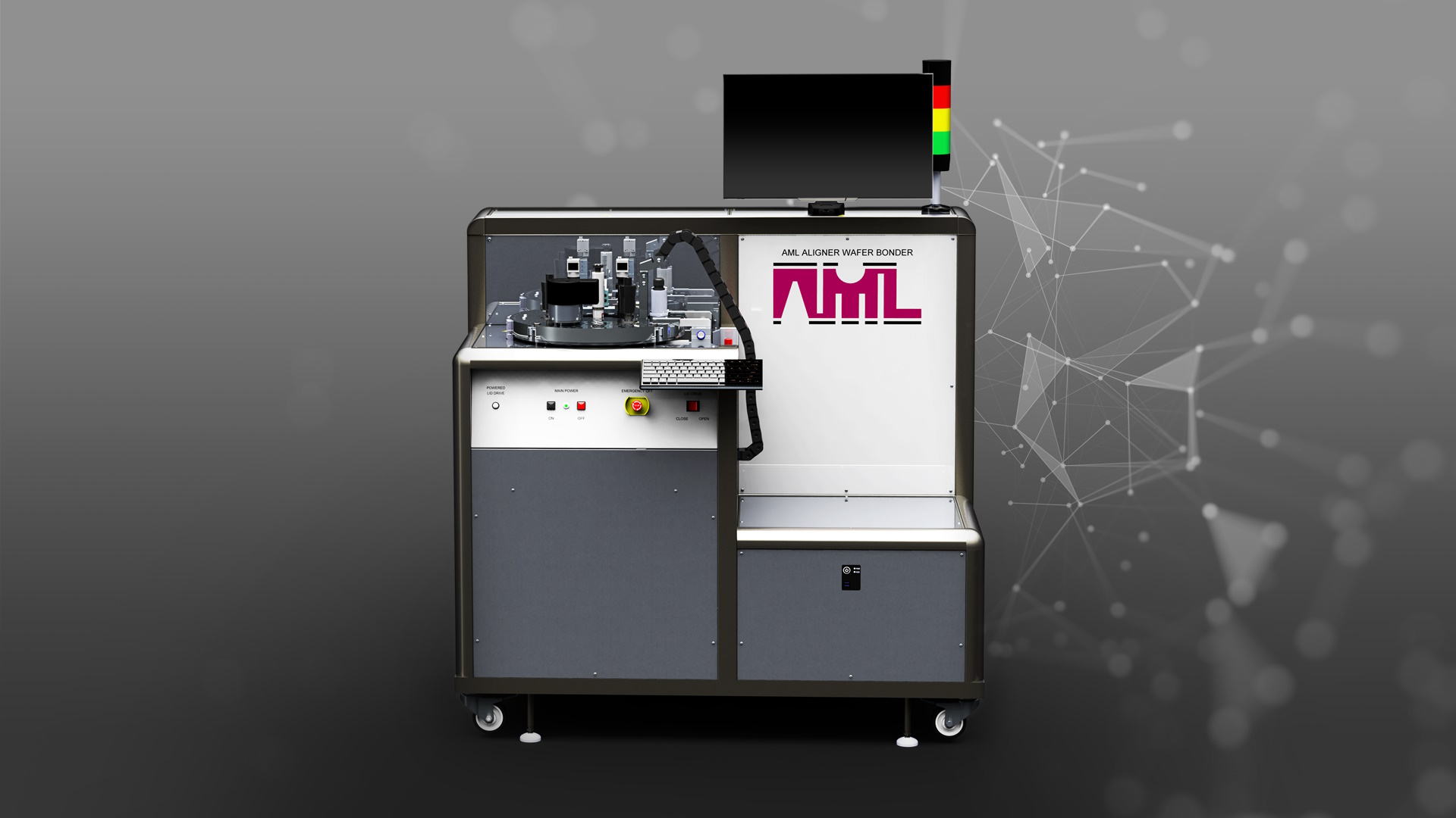
AML 键合机介绍– AWB 04 和AWB 08
AML 键合机应用和市场
AML 键合机应用和市场
Wafer bonding has found many applications in the field of MST, MEMS, III-Vs & ICs and AML machines can be used in the following applications:
High accuracy aligned adhesive bonding “best tool”.
MEMS devices - pressure sensors, accelerometers.
Vacuum encapsulation – ‘best tool on the market’.
1st Level Packaging of devices e.g. silicon microstructures to isolate package induced stresses.
Wafer Scale Packaging – MEMS & IC.
III-V bonding e.g. new high performance LEDs.
3D Interconnects & TSV.
Temporary bonds for handle wafers.
Advanced bonded substrates e.g. silicon-on-glass (SOG).
Smart cut - Layer transfer.
Microfluidics.
AML 键合机应用和市场
AML 键合机应用和市场
Wafer bonding has found many applications in the field of MST, MEMS, III-Vs & ICs and AML machines can be used in the following applications:
High accuracy aligned adhesive bonding “best tool”.
MEMS devices - pressure sensors, accelerometers.
Vacuum encapsulation – ‘best tool on the market’.
1st Level Packaging of devices e.g. silicon microstructures to isolate package induced stresses.
Wafer Scale Packaging – MEMS & IC.
III-V bonding e.g. new high performance LEDs.
3D Interconnects & TSV.
Temporary bonds for handle wafers.
Advanced bonded substrates e.g. silicon-on-glass (SOG).
Smart cut - Layer transfer.
Microfluidics.
The AWB has the versatility to perform aligned:
Anodic, Eutectic, Direct (High & Low Temperature) Glass frit, Adhesive, Solder & Thermo-compression wafer bonding.
New 'Adhesive free' temporary Bonding
Alignment & bonding in one machine
In-situ alignment 1 micron accuracy.
10-6mbar Vacuum to 2bar process gas. UHV Option
Voltage up to 2.5kV.
Temperature up to 560° C.
Forces up to 40kN.
Market leading fast bonding cycle times / high throughput.
Wafer sizes 2"- 8".
In-situ UV cure.
Automatic PC Control & Data acquisition
Live control of all bond parameters or fully automated recipes. All the bonding parameters e.g. current, voltage, integrated charge, temperature, chamber pressure, force, wafer separation, run parameters, recipes, wafer batch No for SPC and event logs are automatically stored in files for graph plotting and trend analysis. Machines can also be networked and remotely interrogated by AML to aid fault finding. Fully automatic recipe, including auto alignment to deskill operation in a production environment.
Alignment:
Manual and auto alignment. In-situ alignment has advantages over other bonders (where alignment is made outside the bond chamber).‘One click’ align and bond. Visible and IR. Image capture for widely spaced 3D alignment marks.
Alignment can be carried out hot or cold:
This eliminates alignment inaccuracies due to thermal expansion & mismatch between wafers, machine parts & platens.
Large wafer separation:
Allows large temperature difference between wafers – ideal for better activation or in-situ oxide reduction via process gas e.g. forming gas. Also allows fast, high vacuum & well defined bonding environment.
In-situ system:
Also enables visual confirmation just before the bonding process that the desired alignment is still being achieved.
Wafer sizes:
2”, 3", 4", 5”, 6” & 8”. (Also chips & odd shaped substrates, but without alignment).
Manipulator:
Enables in-situ alignment of wafers under vacuum and at elevated temperature.
Contact force: up to 40kN provided via manual or motorised hydraulics.
Precise wafer parallelism adjustment.
Alignment accuracy 1 μm.
Optics:
Twin Microscope – camera system with throughthe-lens illumination. Two CCD cameras and side-by-side display of images. Including IR capability. Simultaneous display of wafer separation & bonding force for complete alignment control.
Bonding
Environment:
Vacuum, or process gas. Fully automated dry turbo pumping system ~ 1x10⁻⁶ mbar to 2bar absolute pressure. UHV option
Temperature:
Both Upper & Lower Platens independently adjustable in 1 °C steps. Heating & Cooling rates are programmable. Max Temperature is 560°C.
Electrodes:(for Anodic Bonding)
Full size heated platens for both upper andlower electrodes for better bond uniformity. 0-2.5 kV DC up to 40 mA. Constant current or voltage operation, for improved process control & stress management.
The AWB-04 can bond 3” to 6” wafers and chips
The AWB-08 can bond 6” and 8” wafers
Additional Options:
Auto alignment.
Triple stack bonding tool.
Powered lid.
Pressure control.
CMOS compatible.
High accuracy system for 1μm alignment.
RAD tool for low temperature activated bonding.
In-situ UV Cure.
Motorised X, Y, Ǿ & Z movement.
Image capture.
Process support.
某某婚礼策划
在线QQ:12345678
在线QQ: 12345678
中国某某某有限公司版权所有 沪ICP备12345X78号
COPYRIGHT 2008-2014 WWW.XXXXXX.COM.CN ALL RIGHTS RESERVED
上海市XXXX房产有限公司 沪ICP备020XXXX号 版权所有
Copyright 2016 Global Electronic AG
TeL:0731-85782021 E-mail:Billion.xiao@glb-et.com
湖南格雷柏电子科技有限公司 版权所有
上海市·某某某区·某某某路·某某某大厦·某某层
COPYRIGHT 2008-2014 WWW.XXXXXX.COM.CN ALL RIGHTS RESERVED
上海市XXXX房产有限公司 沪ICP备020XXXX号 版权所有